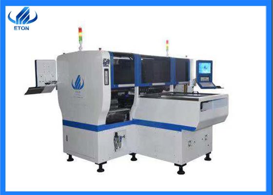
HT-E8D machine is Dual system,dual module multifunctional mounter with high capacity of 80000CPH. It can mount capacitors,resistors,LED3014/3020/3528/5050,IC and shaped components. It applies to power driver,electric board,lens,linear bulb,household appliance and etc..
6.Company profile


7.Our clients

8.FAQ


SMT Patch Process
Incoming inspection => screen printing solder paste (spotting glue)=> patch => drying (curing)=> reflux welding => cleaning inspection => rework
A: incoming inspection =>PCB A surface silk-screen solder paste (dot patch glue)=>PCB> patch PCB surface silk-screen solder paste (dot patch glue). patch =>PCB> drying and reflow welding (preferably only for B surface cleaning =>PCB> detection and rework).
B: incoming inspection =>PCB A surface silk-screen solder paste (spotting glue)=>PCB> patch drying (curing)=>PCB> A surface reflow welding cleaning =>PCB> flip-flop =>PCB =>PCB=>PCB> surface spotting glue/patch curing =>PCB> surface wave soldering inspection and rework)
This process is suitable for PCB A surface reflux welding, B surface wave peak welding. this process is appropriate in PCB SMD assembled on the B surface only if SOT or below the pin.
- Single side mixing process:
A surface silkscreen solder paste (spotting glue)=>PCB> patch =>PCB> drying (curing)=>PCB> reflow soldering =>PCB> cleaning plug-in =>PCB> wave soldering inspection =>PCB> re-repair
- Double-sided mixing process:
B surface patch glue =>PCB> patch =>PCB> curing =>PCB> flip =>PCB =>PCB> wave soldering =>PCB> cleaning and inspection repair
Apply to SMD more than separate components
A surface plug-in (pin bending) B: incoming inspection =>PCB =>PCB> B surface spot patch glue =>PCB> patch cured flip-flop =>PCB> wave soldering inspection and repair
First insert and then paste, suitable for separating components more than SMD components
C: incoming inspection =>PCB A surface silk-screen solder paste =>PCB> patch drying =>PCB> reflux welding plug-in, pin bending =>PCB> flip-flop =>PCB of the B surface spot patch glue, patch curing =>PCB> flip-flop wave soldering cleaning detection =>PCB> rework surface mixed, B surface mount.
D: incoming inspection =>PCB B surface spot patch glue =>PCB> patch cured =>PCB> flip-flop =>PCB A surface silk-screen solder paste patch surface reflow welding plug-in =>PCB> B surface wave soldering cleaning detection =>PCB> rework surface mixing, surface mount. B surface silk-screen solder paste (spotting glue)==>PCB patch ==>PCB drying (curing)==>PCB A surface silk-screen solder paste =>PCB reflow soldering, patch drying = reflow soldering 1(local welding can be used), plug-in, wave soldering 2(if insert components are few ==>PCB, Manual welding can be used)==>PCB cleaning ==>PCB testing ==>PCB rework A surface mount, B surface mix.
- Double-sided assembly process
A: incoming inspection, PCB A silk-screen solder paste (patch glue), patch, drying (curing), A surface reflow welding, cleaning, flip plate; PCB silk-screen solder paste (patch glue), patch, drying, reflow welding (preferably only for B surface, cleaning, testing, rework)
This process is suitable for PCB with large SMD such as PLCC on both sides.
B: incoming inspection, PCB A surface silk-screen solder paste (spot patch glue), patch, drying (curing), A surface reflow welding, cleaning, flip plate; PCB surface spot patch glue, patch, curing, B surface wave soldering, cleaning, testing, rework) this process is suitable for reflow on PCB surface.
contact
Name:Brynn
Email :Brynn@eton-mounter.com
WeChat:13802252825
Telephone:138 0225 2825

 Ваше сообщение должно содержать от 20 до 3000 символов!
 Пожалуйста, проверьте свою электронную почту!
  Ваше сообщение должно содержать от 20 до 3000 символов!
 Пожалуйста, проверьте свою электронную почту!


